
Murali Srinivasa on how PCBs are made and why India lags

As you all know, at The Daily Brief, we have been writing about electronic components like semiconductors, PCBs, and a lot more for some time now. When we wrote about the manufacturing of printed circuit boards (PCBs), Murali Srinivasa from Lion Circuits replied to us.
We thought it would be nice to learn from him about how PCBs work. Here are some of the things that stood out to me in our conversation.
You can also listen to this on Spotify and Apple Podcasts.
The board inside your phone is a 60-floor building
Everyone talks about chips, but every chip needs something to sit on, something to connect it to other components, something to carry electrical signals from one place to another. That something is a printed circuit board. Everything from your phone, to your laptop, to your TV remote, and even the engine control unit in your car, has at least one PCB.
The simplest way Murali explained it was through an analogy with a building’s electrical system. You have a main control panel, you have bulbs on different floors, and you have wires running from the panel to each bulb. A PCB does essentially the same thing, except it shrinks the whole setup by a factor of a thousand or more. The wires become copper tracks etched onto a surface, the bulbs become LEDs or sensors, and the control panel becomes a semiconductor chip.
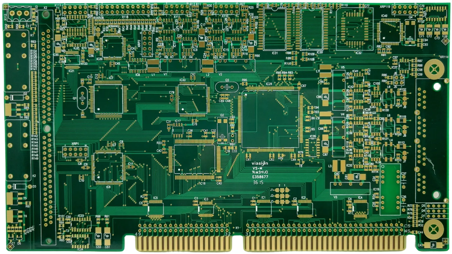
But here’s what surprised me. The PCB inside your phone is less a flat board with some tracks running across it, and more a skyscraper.
Murali said that a typical smartphone PCB is about one millimetre thick, roughly the thickness of a credit card. But inside that one millimetre, there are fifty to sixty layers stacked on top of each other. Each layer is like a floor in a building, with its own copper tracks, its own electrical connections. A signal can start at the bottom and travel to the top through tiny plated holes that act like staircases between floors. So when you’re holding your phone, you’re holding a sixty-floor building compressed into the thickness of a credit card.
The fifty-micron problem
Not all PCBs are sixty-layer skyscrapers, of course. There’s a whole spectrum. Your TV remote has a simple single-layer board. Some devices use double-layer boards, with tracks on top and bottom. Then there are multi-layer boards with four, six, eight, or twelve layers, the kind you find in car engine control units. And at the extreme end, you have phones and smartwatches with fifty or sixty layers. The more layers you have, the harder it is to make.
When you’re making a multi-layer board, you manufacture each inner layer separately, then press them all together like a sandwich. After that, you drill holes through the stack to connect the different floors. The problem is that once you’ve pressed all the layers together, you can’t see the inner ones anymore. You’re drilling blind, trusting that everything aligned perfectly.
And how perfect does it need to be? He told me that if a layer shifts by just fifty microns during pressing, the entire board becomes scrap. Fifty microns is half the thickness of a human hair. You’re building something with sixty floors, compressing it into one millimetre, and if any floor is off by half a hair’s width, the board goes in the bin.
Why money alone can’t solve this
This kind of precision is why PCB manufacturing isn’t just about having the right machines. He used a phrase that stuck with me: tribal knowledge. It’s the knowledge that exists only within people who do the work, year after year. It’s not in any manual, it’s not taught in college, and it can’t be bought from a consultant. It lives in the hands of people who’ve spent years figuring out why the same machine, same chemical, same process produces different results on different days.
He put it this way: if someone gave him ten thousand crore rupees today and asked him to build a jet engine in six months, the same timeline Boeing uses, it would be impossible. Not because of the money, but because that kind of knowledge doesn’t transfer through bank accounts. It transfers through people, slowly, over the years.
This is also why China is so far ahead of us in PCBs. In the early 2000s, American companies didn’t just move orders to China. They moved engineers who taught Chinese factories how to build things. The tribal knowledge that had accumulated over decades got transferred, person by person. India, focused on IT and services, missed that transfer almost entirely.
There’s a lot more in our conversation - how India was actually ahead of China in the 1980s, why we became a net importer of copper, what it takes to go from making 150-micron tracks to 25-micron tracks, and what needs to happen for India to build a real PCB industry.
If you have made it this far, you will enjoy the full conversation for sure. Check it out here:
Apple in China: The Capture of the World's Greatest Company by Patrick McGee
The above book is the perfect example of engineers from USA going to China to teach manufacturing and then loosing the manufacturing edge and the knowledge required for manufacturing as the Chinese developed the manufacturing knowledge further.
Wish the podcast host dug a bit deeper.